Driving Efficiency and Reliability
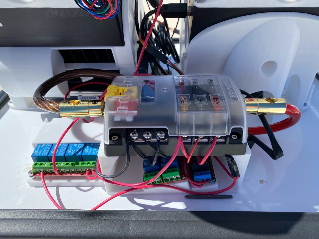
A LaserSETI instrument is full of computers, sensors, and other electronics, and hence it’s also full of wires. Each wire has to be cut to length, connected firmly, and worked around carefully when performing any other operation on the instrument.
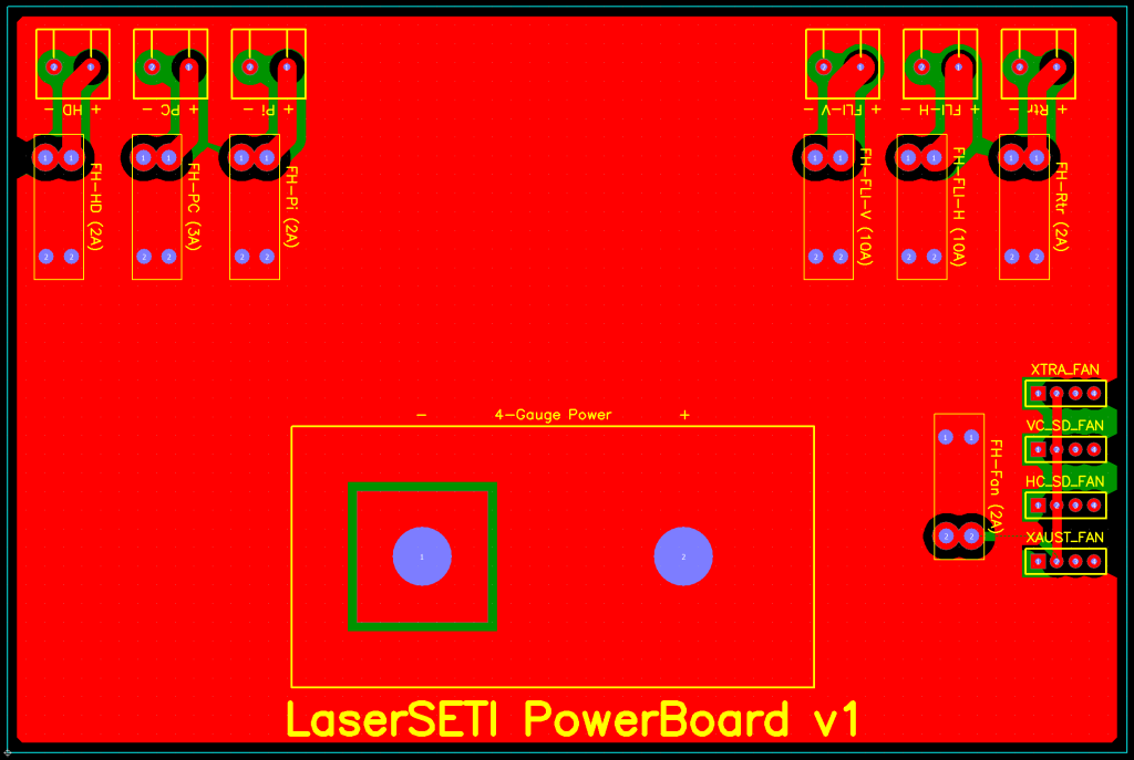
It’s therefore very exciting that we’ve designed a custom PCB (printed circuit board) that can reduce all that complexity, effort, and risk. Thanks to today’s modern electronics ecosystem, it’s easily outsourced and since it replaces existing COTS (commercial off-the-shelf) components, these benefits add nothing to the cost of an instrument.
We’re not quite done making sure every need and clearance is accounted for, but we’re close. Since these traces will carry a decent amount of current, however, we have at least validated the current flow, trace width, copper thickness, and resulting temperature increase is very well within limits (credit: PCB Trace Width Calculator). We want both the boards to be super reliable for the long term, even when it gets hot inside the instrument on some days or at some locations.